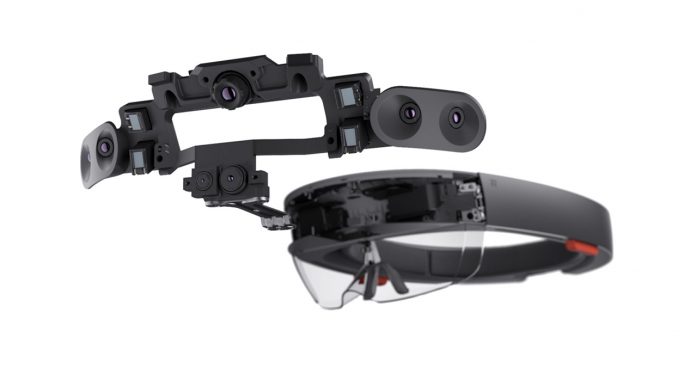
The special HPU has been designed to take most of the load from the CPU and GPU so that they can focus on launching apps and displaying holograms. At the Hot Chips conference in California this week, devices engineer Nick Baker told us exactly how that works.
Holographic Processing Unit Specifications
According to The Register, the device is a TSMC fabricated 28nm coprocessor. It has 24 Tensilica DSP cores, 65 million logic gates, 8MB of SRAM and 1GB of DDR3 RAM. All of this means that the HPU can handle up to a trillion calculations per seconds on its own, in a 12-12mm BGA package. Just as impressive as the size is the power draw of the hardware. Allegedly, it uses less than 10W from the power supply to handle environment scans and gestures. It also supports PCIe and standard serial interfaces, and well as ten custom instructions to speed up AR algorithms.
Full HoloLens Specifications
The information means that we now have the complete specifications for the HoloLens, as listed below:
OS: 32-bit Windows 10.0.11802.1033 CPU: Intel Atom x5-Z8100 Airmont, 1.04GHz 64-bit capable HPU: TSMC-fabricated 28nm coprocessor, 24 Tensilica DSP cores, 8MB SRAM, 1GB DDR3 RAM GPU: HoloLens Processing Unit (HPU) Dedicated Video Memory: 114 MB Shared System Memory: 980 MB RAM: 2GB Storage: 64GB (54.09 GB available) App Memory Usage Limit: 900 MB Battery: 16,500 mWh Camera Photos: 2.4 MP (2048×1152) Camera Video: 1.1 MP (1408×792) Video Speed: 30 FPS
The augmented reality headset is starting to look very impressive considering its lack of power supply. The addition of the holographic processing unit accelerates algorithms by up to 200 times when compared to pure software. Developers first got their hands on the HoloLens in March, and it’ll be interesting to see just how far they can push the unit.


